
 中文摘要:
中文摘要:
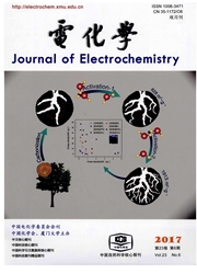
铅锡合金的准二维电沉积物具有伪共晶.固溶体双层结构.研究表明,这种奇特的结构是由生长界面上电流密度自发变化引起的.当生长界面处于整个沉积物前端时,电流密度大,铅和锡共同沉积形成伪共晶组织;当生长界面处于整个沉积物后端时,电流密度小,铅沉积成为主要反应,此时沉积物是含铅较多的固溶体组织.
 英文摘要:
英文摘要:
A two-layered structure of eutectic-solid sulotion is formed in the microstructure of Pb-Sn alloy obtained from quasi-two-dimensional electrodeposition. It is showed that this unique structure is caused by the variation of the current density on the growth interface. When the interface is located in the front of the whole deposits, the current density is high. So the Pb and Sn can deposit together and the eutectic texture forms. When the interface is in the rear of the whole deposits, the current density is low. At this moment the electrodeposition of Pb is the dominant reaction, and the Pb-based solid solution appears.
 同期刊论文项目
 同项目期刊论文
 期刊信息
期刊信息
